Miniaturized PCB Assembly for Wearable Devices: Trends and Techniques
- Mefron Technologies
- Jun 7, 2025
- 2 min read

As wearable technology continues to expand across healthcare, fitness, lifestyle, and industrial applications, the demand for miniaturized and high-performance electronics has grown significantly.
At the core of these devices lies the Printed Circuit Board (PCB), and the complexity of assembling miniaturized PCBs has become a crucial area of focus for manufacturers. In this blog, we explore key trends and techniques shaping miniaturized PCB Assembly for wearable devices.
Why Miniaturization Matters in Wearables
Wearable devices are defined by their portability, comfort, and integration into everyday life. Whether it's a smartwatch, fitness band, medical patch, or smart clothing, space is limited and performance expectations are high. This makes PCB Assembly Services for wearables uniquely challenging. The PCBs must be compact, lightweight, power-efficient, and durable enough to withstand frequent movement, moisture, and temperature variations.
Emerging Trends in Wearable PCB Assembly
Flexible and Rigid-Flex PCBs
Traditional rigid boards are being replaced with flexible and rigid-flex PCBs to accommodate dynamic form factors. These allow PCBs to bend and twist without damage, which is ideal for wrist-worn or body-mounted devices
High-Density Interconnect (HDI) Technology
HDI PCBs enable a greater number of components in a smaller footprint by using microvias and multiple layers. This is essential for wearables that demand multifunctionality without increasing size.
Component Integration and Miniaturized Packages
The shift toward smaller and more integrated packages such as CSP (Chip Scale Packages) and 0201-size passive components enables compact board designs while maintaining performance.
Wireless and Sensor Integration
Wearables are increasingly being designed with embedded Bluetooth, NFC, and a range of sensors (ECG, temperature, accelerometers), requiring precise placement and shielding in the PCB assembly process
Techniques for Effective Miniaturized PCB Assembly
Surface Mount Technology (SMT):
SMT is widely used in wearable electronics to mount components directly onto the board surface, enabling compact and efficient layouts.
Automated Optical Inspection (AOI):
As component sizes shrink, traditional visual inspection becomes less viable. AOI ensures defect detection in high-density assemblies, improving quality and yield.
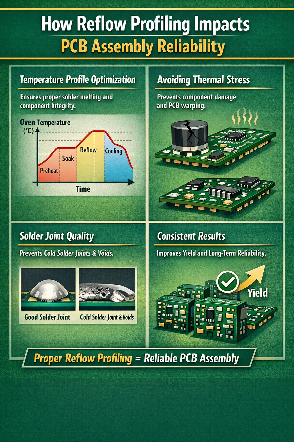
Precise Soldering and Reflow Profiling:
Miniaturized components require tight control over solder paste application and reflow temperatures to avoid issues like tombstoning or cold solder joints.
3D PCB Design Tools:
Advanced CAD software with 3D modeling allows engineers to simulate compact layouts and mechanical constraints, reducing prototyping cycles and enhancing reliability.
Conclusion
As the wearable tech market continues to grow, success in product development hinges on the ability to deliver reliable, compact, and high-performance PCBs.
At Mefron Technologies, our PCB Assembly Services are tailored to meet the unique challenges of wearable devices—from flexible PCB handling to fine-pitch component placement and testing. Partner with us to bring your next-generation wearable innovations to life with precision and scalability.


Comments